Packaging
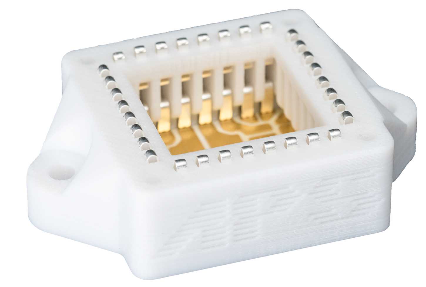
This research area concerns itself with the development of new packaging techniques and the design of advanced power modules. The goal is to reach outstanding functionality and reliability by using state of the art technologies, materials and architectures.

Packaging for Wide Bandgap Semiconductors
While devices using wide bandgap semiconductors are already on the market they generally use packaging technologies inherited from older silicon devices. This hinders their performance and does not allow them to reach their full potential. The APS is working on improving packaging to enable the new devices to work at higher voltages, higher frequencies and higher temperatures while achieving higher density and better reliability than previously possible.